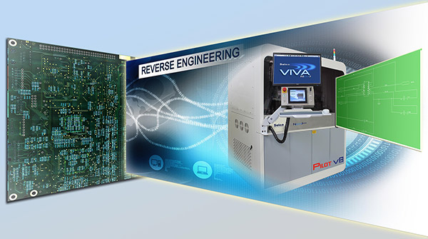
reverse-engineering
WHAT IS REVERSE ENGINEERING
In the Electronics industry, the concept of Reverse Engineering (hereinafter referred to as “RE”)represents the process used to understand how a device, object, or system has been designed: it allows redesigning the technical construction through the analysis of its structure, function and operation.
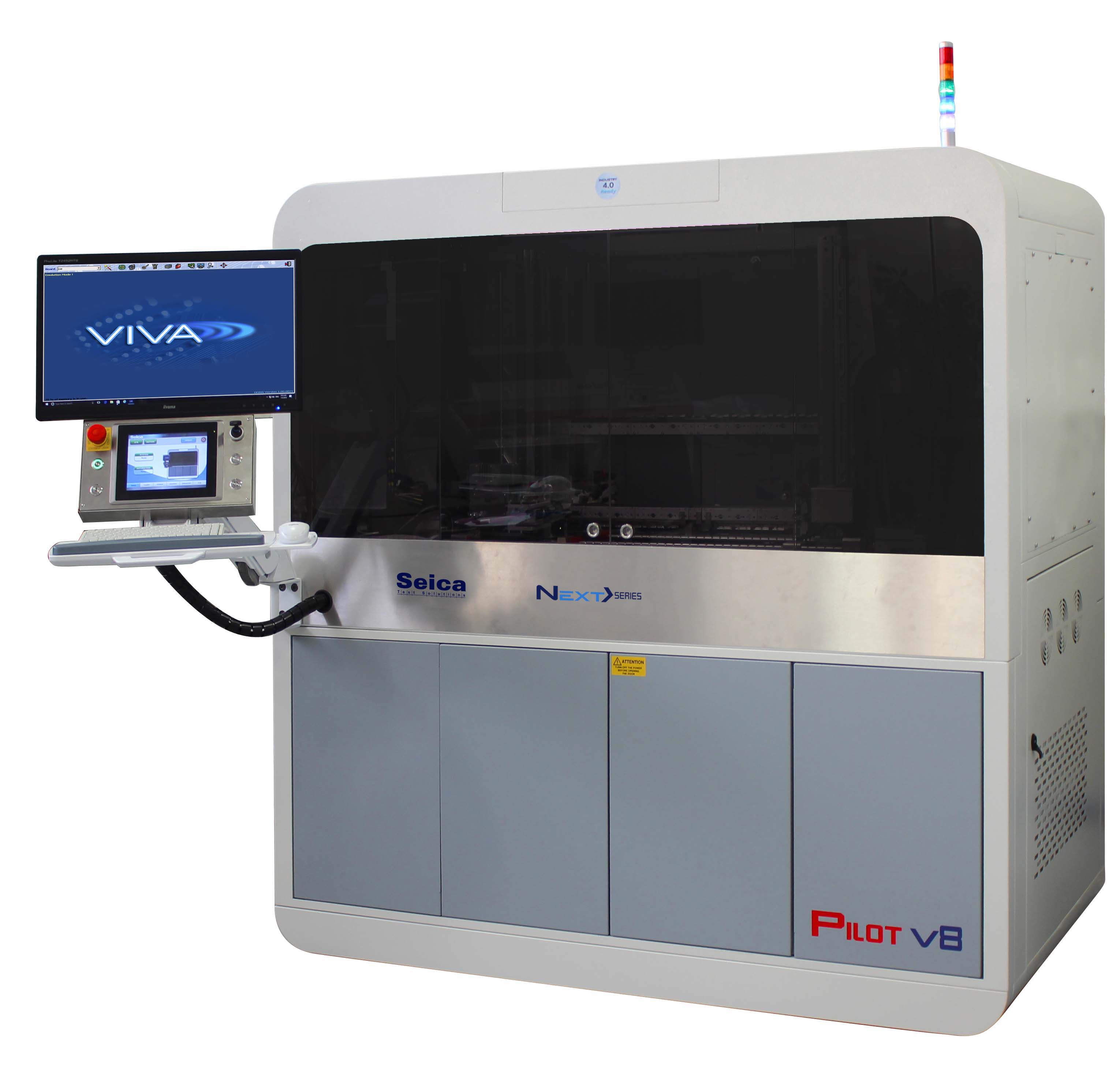 The best solution to automatize this long process for Reverse Engineering is the Pilot V8 Next Series tester by Seica. The PCB accessibility on both sides is a preliminary and mandatory condition to fully rebuild the netlist because this is the only way to learn connections between SMD components on opposite sides. The vertical architecture is the best mechanical damping because board vibrations are not increased by the force of gravity. Sophisticated but easy-to-use algorithms drastically decrease the total amount of tests, reducing the total reverse time and costs. The rebuilt data are ready to use to generate a test program by automatic procedures.
1. BOARD ANALYSIS
Thanks to multiple inspection and analysis techniques, the VIVA software may operate both on mounted and bare boards.
The reverse engineering can have a destructive or a non-destructive approach. The first method will destroy the device during the test procedure, while the non-destructive process retains full functionality of the device under test after the analysis. The Pilot V8 Next Series> tester by Seica features a non-destructive method, although the following exceptions must be taken into account and solved:
1) Microchips with BGA packages with the pins below the component, because it is necessary to expose the pads.
2) Components with no accessibility.
3) Protective coating that is a thin polymeric film applied to a printed circuit board (PCB).
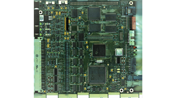
The result of the netlist autolearning procedure depends on the real accessibility of the probes on the test points. It is possible to analyze the following types of electronic boards:
– Bare board: this condition provides a complete and reliable learning of all the netlists on the PCB. Moreover, the check of the data learned is relatively easy and fast.
– Partially mounted board: to enhance the accessibility and minimize the subsequent manual operations, it is recommended to remove those components which prevent the access to some pads.
– Fully assembled board: in this case, the limited accessibility to the pads may require the execution of manual netlist learning using the dedicated tools available in the VIVA software.
2. AUTOLEARNING: DUAL SIDE BOARD DIGITALIZING
 The CCD color cameras, available on each side of a Pilot V8 Flying Prober, digitalize two detailed images of the top and bottom sides of the board. Seica has developed several manual and automatic routines that identify the XY location coordinates using the built-in AOI system. There are four modes for auto-learning all the points and components of a board: Manual, Automatic, Connector and Component. This technique reproduces the full layout and it is useful for data processing and analysis, either online (auto-learn) in the system or offline (digitizer) on a remote PC.
3. NETLIST LEARNING
The first step is to manually identify at least one GND point. Similarly, the user can determine the VCC point if it is useful for the netlist analysis. Once the user has classified the GND signal, the “netlist learning” process on the Flying Prober can start with the FNODE macro.
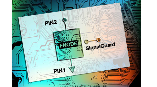
FNODE
Seica employs a proprietary dynamic impedance measurement method designated as FNODE, which acquires the net signature of an analog dipole. This powerful test method is used to measure the dynamic impedance of an unknown dipole to recognize and separate all the nets of a mounted board. From that, it creates a suitable number of continuity tests.
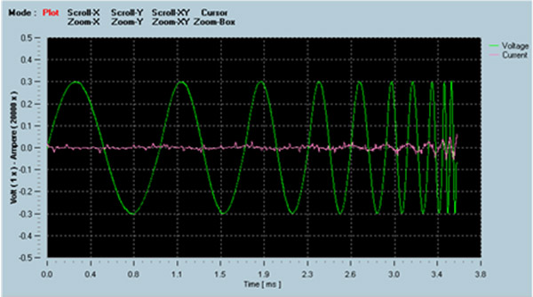
Since each dipole of the UUT is unknown, an “auto-learn” of the golden board is used to acquire the behavior of the dipole over a broad frequency range. A signal generator applies a frequency sweep to pin1 while pin2 is connected to GND. In green, the voltage applied between the net under test and ground, in magenta the current signature of the net. The typical input signal amplitude is 0.2 V to be below the P-N transition threshold and to avoid nonlinear distortions as well as to avoid guarding (electrically isolating the net environment to perform an individual measurement on a single component). The FNODE measures the current which flows into the dipole and, in each case, the amplitude and the phase for each net is stored by the test program. The FNODE is a purely passive measurement procedure, with no power on the UUT. 
The advantages of FNODE are easily summarized:
– It does not need any CAD data and no manual debug is necessary
– The auto-learn process is fully automatic and creates a full shorts test higher fault coverage than the traditional adjacency test. Moreover, many in-circuit measurements can be avoided without decreasing test coverage.This procedure utilizes a DSP-based (Digital Signal Processor) multi-function instrument, which digitizes the generated and measured signals. The acquired data enable the almost simultaneous execution of multiple, high-speed tests, because all of the test models are “hardware-emulated”, substantially increasing the test throughput.
CONTINUITY MACRO
If two or more nets have the same current signature, the next step is to execute the continuity test. The main goal of the CONTINUITY macro, optimized to work in sets of 1000 tests each, is to group the test pads belonging to the same net. This procedure is also capable of detecting as separate nets the signals connected to low impedance (e.g. inductors, resistances at 0 Ohm …) when belonging to two-pin components regularly declared in the graphic environment Edit Board of the VIVA software.
PWMON
At this point, it is necessary to acquire the signatures/functions of the digital components. Once the GND and VCC inputs have been identified, the UUT is powered on to execute the Power Monitor (PWMON). It is possible to measure the current needed to produce logic 0 or logic 1 on each node (input pin of a digital component). This way, the threshold is learned and the system can recognize a possible error on a net. Using this method, a “golden board” is not necessary but strongly recommended.
The advantages of PWMON are summarized as follows:
– It is a vectorless method to test ICs in a powered up condition.
– It can be generated without CAD data.
– It does not require manual operations, since it is a fully automatic procedure and it is independent of the UUT initialization conditions (when the UUT is powered on).
4. TEST PROGRAM CREATION
Once the netlist learning procedure has been completed, along with the possible manual connection of some nets, the tast carried out may be employed to create a test program for repair activity purposes, and/or create the data to be employed to rebuild the board schematics.